
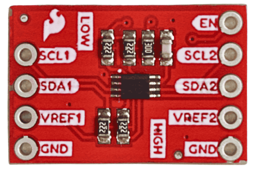
The PCA9306 module is a two-way I2C/SMBus voltage-level translator using the PCA9306 IC. This PCA9306 module is built to connect low-voltage controllers like 1.0 - 3.3V with higher-voltage devices up to 5V. It uses MOSFETs to handle open-drain signals, which is perfect for two-way communication protocols like I2C. The board includes built-in pull-up resistors, allowing for easy communication between different voltage systems. The detailed specifications are given in the attached PCA9306 module datasheet.
What Is The PCA9306 Module?
The PCA9306 provides an interface between two different operating voltages; it also allows users to connect multiple lower-voltage devices to a higher-voltage bus. The use of MOSFET transistors in the design provides a high level of reliability and is very effective for managing open-drain signals, making it suitable for both applications requiring international and domestic standards within telecommunications and networking.
The PCA9306 comes fully assembled and includes all required components for the user to simply plug in their own controllers/devices. Users do not have to worry about sourcing external resistors, diodes or capacitors as these have already been installed as part of the assembly process.
The compact PCA9306 breakout board design is an ideal solution for prototyping and production applications where a low-power consumption mixed voltage interface between multiple devices on the same bus or line is needed.
Why Choose the PCA9306 Module
The PCA9306 module remains a viable solution as a robust, cost-effective solution for the task of I2C bus voltage-level translation in mixed-voltage embedded applications. This is owing to the advantages of the PCA9306, which include the ability for the module to be bidirectional, support a wide range of voltages, and require fewer peripheral parts, thus becoming the best interface solution for the latest 3.3-volt microcontrollers as well as 5-volt peripheral equipment. While working with the PCA9306 breakout board, getting a clear understanding of the PCA9306 pinout, circuit diagram, and PCA9306 operation is important.
PCA9306 Pinout Configuration and Pin Functions
The image shows the pinout of the PCA9306 Logic Level shifter module.
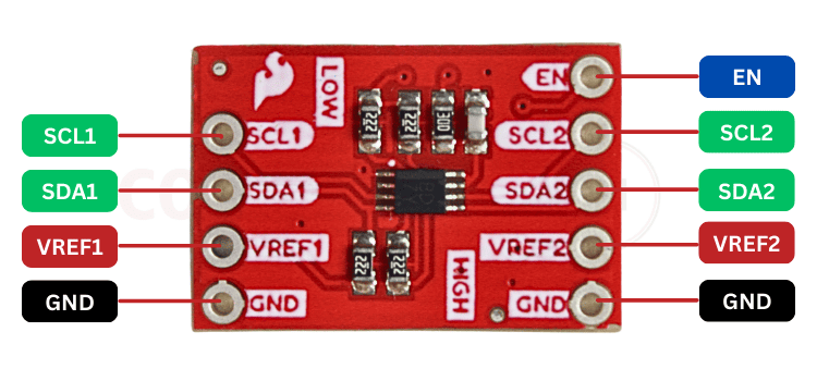
The table showing the pins and their explanation of the PCA9306 module
Complete PCA9306 Pin Description
| Pin No. | Name | Description |
| 1 | VREF1 | Low-side reference voltage (1.0–3.3V domain) |
| 2 | SDA1 | Low-side I2C data |
| 3 | SCL1 | Low-side I2C clock |
| 4 | GND | Ground |
| 5 | EN | Enable input for the translator |
| 6 | VREF2 | High-side reference voltage (up to 5V domain) |
| 7 | SDA2 | High-side I2C data |
| 8 | SCL2 | High-side I2C clock |
Key Features and Specifications of PCA9306 Module
The PCA9306 module offers several technical advantages that make it the preferred choice for I2C bus voltage translation in embedded systems:
- Bidirectional I2C/SMBus communication
- Supports 1.0V to 5V level translation
- MOSFET-based pass-gate architecture
- Up to 400kHz I2C operation
- Low propagation delay
- Enable pin for power-down control
- Compatible with open-drain and bidirectional signals
- Minimal external components required
Manufacturer of PCA9306 Level Shifter
Implementing the PCA9306 module in I2C bus applications requires careful consideration of pull-up resistor values and capacitive loading. The PCA9306 IC is manufactured by
PCA9306 Module Equivalent
If you are looking for an equivalent or drop-in replacement for PCA9306, there are several ICs in the market, LSF0102 and TCA39306.
Practical Applications of PCA9306 Module
The PCA9306 breakout module finds extensive use in various embedded systems and electronics projects:
- Mixed-voltage embedded systems
- Sensor interfacing (5V sensors with 3.3V MCUs)
- IoT nodes and gateways
- Robotics controllers
- Multi-voltage testing/prototyping benches
- Power-sensitive portable devices